Historial Development of PLD
Albert Einstein postulated the stimulated emission process in as early as 1916. The first optical master using a
rod of ruby as the lasing medium was, however, constructed in 1960 by Theodore H. Maiman at Hughes Research
Laboratories, a lapse of 44 years. Using laser to ablate material has to be traced back to 1962 when Breech and
Cross [1], used ruby laser to vaporize and excite atoms from a solid surface. Three years later, Smith and Turner
[2] used ruby laser to deposit thin films. This marked the very beginning of the development of the pulsed laser
deposition technique.
However, the development and investigations of pulsed laser deposition did not gather the expected momentum.
In fact, the laser technology was immature at that time. The availability of the types of laser was limited;
the stability output was poor and the laser repetition rate was too low for any realistic film growth processes.
Thus the development of PLD in thin film fabrication was slow comparing with other techniques such as MBE
(Molecular Beam Epitaxy),
which can produce much better thin film quality.
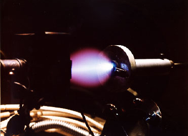
A plasma plume inside a PLD chamber
The rapid progress of the laser technology [3,4], however, enhanced the competitiveness of PLD in the following
decade. The lasers having a higher repetition rate than the early ruby lasers made the thin film growth possible.
Subsequently, reliable electronic Q-switches lasers became available for generation of very short optical pulses.
For this reason PLD can be used to achieve congruent evaporation of the target and to deposit stoichiometric thin
films. The absorption depth is shallower for UV radiation. Subsequent development led to lasers with high efficient
harmonic generator and excimer lasers delivering powerful UV radiation. From then on, non-thermal laser ablation
of the target material became highly efficient.
Pulsed laser deposition as a film growth technique has attained its reputed fame and has attracted wide spread
interest after it has been used successfully to grow high-temperature superconducting films in 1987. During the
last decades, pulsed laser deposition has been employed to fabricate crystalline thin films with epitaxy quality.
Ceramic oxide, nitride films, metallic multilayers, and various superlattices grown by PLD have been demonstrated.
Recently, using PLD to synthesis nanotubes [5], nanopowders [6] and quantum dots [7] have also been reported.
Production-related issues concerning reproducibility [8], large-area scale-up [9] and multiple-level have begun
to be addressed. It may start up another era of thin film fabrication in industry.
References:
- F. Breech and L. Cross, Appl. Spect.16, 59 (1962)
- H.M. Smith and A.F. Tuner, Appl. Opt. 4, 147 (1965)
- C.K.N. Patel, Phys. Rev. Lett.12, 588 (1964)
- J.E. Geusic, H.M. Marcos and L.G. Uitert, Appl. Phys. Lett. 4, 182 (1964)
- Y. Zhang, H. Gu, and S. Iijima, Appl. Phys. Lett. 73, 3827 (1998)
- D.B. Geohegan, A.A. Puretzky, and D.L. Rader, Appl. Phys. Lett. 74, 3788 (1999)
- T.J. Goodwin, V.L. Leppert, S.H. Risbud, I.M. Kennedy, and H.W.H. Lee, Appl. Phys. Lett. 10, 3122 (1997)
- J.T. Cheung, I.M. Gergis, J. James and R.E. DeWames, Appl. Phys. Lett. 60, 3180 (1992)
- J.A. Greer and H.J. Van Hook, Mater. Res. Soc. Symp. Proc. 191, 171 (1990)

